Not much has been happen to graphene in these dog days of summer, when all sane journalists go to earth. With few politicians to run around making daft statements, and much of Europe shut down, publications have a hard time finding anything serious to write about. One consequence of the silly season is that, just as Friday is a good day to bury news during normal times, August is a fine time to put out stuff that you don’t really want trumpeted to the heavens.
Can this really be why the University of Manchester chose the holiday season to trickle out the news that it has "appointed a Business Development and Strategy Director for graphene to attract some of the world’s biggest companies to partner with the National Graphene Institute”?
This is, after all, the university that gives lab space to none other than Andre Geim, “inventor” and cheerleader for graphene, and the man who, a week or so before the latest announcements, said in a programme on BBC Radio 4 that the taxpayer funded his research, so he felt no great urge to patent his work or to rush to make money out of it. (The BBC also gave air time to Geim’s ideas in a recent Radio 4 Profile of the frog levitating Nobel laureate.) If the taxpayer backed him, Geim argued, then he owes it to society to publish what he does openly for anyone to develop as they see fit.
Perhaps it is just the conspiracy theorist in us that looks for ulterior motives behind the absence of Geim’s name in Manchester’s announcement that Nathan Hill, another lapsed physicist, is to be Business Development and Strategy Director. (It can be hard to tell these days if those capital letters deliberate, and a job title, or sloppy editing.) The press release tells us that the appointment “marks a pivotal phase in the engineering and commercial development of graphene as an industrial material”.
Hill certainly has done time in a business that grew out of university research. He worked at Oxford Instruments “where, as a Managing Director, he worked on thin film and bulk superconductors and semiconductor materials and devices”, all good grounding for work on graphene. Over on the website of another of Hill’s businesses, Qi3, with a focus on “providing hands-on expertise in all aspects of marketing technology-based products, from strategy to implementation”, we read that his skills “are in sales, sales management, product marketing, strategic portfolio management, acquisitions and general management in export markets”.
Those skills probably explain why Manchester reeled him in. The job there seems to be to bring in businesses to work with the local researchers. Hill’s first job there, we read, “will be to set up a graphene Industry Club and a number of strategic partnerships with major companies”. At a strategic level, the job will be “focus on strategy and business development for the £61m National Graphene Institute”.
These days governments throw money like that at research in the expectation of a payback. They don't invest in research for its own sake. There has to be impact, as they tirelessly proclaim. So there has to be someone in there countering the woolly minded liberal thinking of all those scientists who do research fore the fun of it and for the greater good of mankind, rather than for the money that they could make out of it.
22 August 2013
Manchester does the business with #graphene
06 August 2013
Share pushers discover #graphene
You know that a technology is fashionable when share tippers deploy it to rope in suckers. Last week brought no fewer than three invitations to read reports offering insider information on how to make money by investing in graphene businesses. Fortunately, not all of these invitations turn out to be from operations that, a century ago, would have purveyed snake oil.
Let’s get the good guy out of the way first: Cientifica, the self styled "leading authority on rational technology information", has put out Investing in Graphene. (With luck the PDF link will work for you.) This is worth reading for one section alone, the bit where, unlike many reports on graphene, it looks back at previous carbon bubbles. In particular, it says of C60 and nanotubes:
The new brief report from Cientifica gives a blow-by-blow account of attempts to commercialise nanotubes, something rarely mentioned by graphene's advocates, who don't seem to know much history. (It could also have used as a carbon-free example, high-temperature superconductors, which many years after it collected a Nobel Prize almost within months of discovery, has yet to live up to the promise of changing the face of energy transmission.)“As often happens with nanomaterials, realizing any return on the huge investment in production capacity proved far more difficult than people would ever imagine. Investors lost substantial amounts of money in venture-backed companies such as C60 and Carbon Nanotechnologies Inc. (CNI), while industry giants such as Bayer struggled to sell their product for over a decade before recently throwing in the towel.”
Cientifica goes on to say that graphene could be different because “Unlike previous carbon nanomaterials, graphene appears to lend itself to processing either through CVD grown sheets of the material or by dispersing nano platelets of graphene in various other media to produce inks paints and coatings.” The fact that the report doesn’t bother to explain what CVD stands for – chemical vapour deposition, of course – tells us that this document is not intended for your average “day trader”. (Actually, maybe it was just an editing lapse, one of several in the document.)
Riding the hype cycle
Given the space available, Cientifica’s document is good on its description of the “Nanomaterials Hype Cycle”. It also goes on to offer advice on assessing graphene producers.It also makes the sound hype-cutting observation that “no one buys graphene but they do buy batteries, composites, sensors and touch screen components”. Any serious investor might well read this and move on to more promising ways of making money. Fair enough, Cientifica is not a share tipster.“When looking at graphene producers there are a few simple rules to help pick the winners. The ones to survive and prosper will not necessarily be the ones with the best technology, in early stage materials production its all about top line revenue and keeping ahead of the chasing pack.”
The same is not true of two other outfits that popped up with sponsored ads on a graphene news site inviting visitors to sign up for newsletters and reports on graphene. Normally wary if such invitations, this one appeared on a site that I have usually considered reliable, so I clicked the buttons to get these free reports.
The process also signed me up for daily newsletters. You might think that these might have something to do with graphene. They were really more interested in telling me of the value of investing in silver and gold, important materials, maybe, but hardly new to the world of technology.
One of these reports has the grandiose title How to Invest in the Graphene Revolution. Not really, it is just a share tipster pushing a mining company. The odd bit is that the company involved, Northern Graphite Corp., does not push itself as a graphene business, the word does not even feature in its latest “Corporate Update”.
This is not surprising given the other markets for graphite. Take the lithium-ion battery. The company tells us that “Graphite demand in Lithium ion batteries was estimated at 44,000 tonnes in 2008 or about 10 per cent of the flake market.” So why try to make strange claims about unknown markets that now need small amounts of graphite when there are already people queuing up to buy tonnes of the stuff?
Mines of misinformation
Northern Graphite is really in business to develop a graphite mine, so the compeny, like graphene's fans, in the carbon business, so it isn’t that dumb that it eschews all reference to the magic material. After all it may well come up in a web search. The site has a brief and measured description of Graphene with links to other sources of information.Northern Graphite has even put a toe in tyhe graphene water and provided material to "an eminent professor in the field at the Chinese Academy of Sciences who is doing research making graphene sheets larger than 30cm2 in size using the graphene oxide methodology". But that is as far as it goes in trying to enthuse potential investors.
The people at Northern Graphite would probably go along with Cientifica’s analysis. It would be interesting to know what they make of the attentions of the share tippers. And why did those tippers decide that possible sales of graphene is a better sales pitch than a large and growing existing market for batteries or fuel cells?
There are others out there claiming to offer advice on how to make loadsamoney out of graphene. One of these sites has a link from the text “What’s the only graphene investment on earth worth considering right now?” The get rich quick mob will be disappointed if they follow the link it delivers the report Massive Breakthrough For Graphene Investors.
The report turns out to be as misleading as the title and the link. For a start it would seem to fly in the face of the boosters of mining companies. It warns “there's no good way to invest in graphene - or the graphite carbon it's made from - as a commodity”.
What no breakthrough?
As well as missing the promised advice on “the only graphene investment on earth worth considering right now”, this report also has no mention of massive breakthroughs for graphene investors. Instead it offers mostly sane warnings. As it says “finding the right vehicle to catch the graphene wave will be a challenge – requiring both patience and close attention”.Here’s our own personal tip on who will make early money on graphene, look no further than the people who make the equipment that is in demand among people who are looking for possible applications of graphene. Then again, these are often small companies that also sell to other bits of the R&D community.
Were it not for some of the promises made on the website – including the claim that “Doctors will soon use it to create implants that will end brain disease...” – the report, minus its title, is sound advice that is mostly in line with Cientifica’s careful approach. Perhaps the idea is just to sign up subscribers to its services.
Finally, we came across a new report from Research and Markets that makes no claim to offer investment advice. And if information is worth what you pay for it, there should be plenty of opportunities to earn money after reading The Global Market for Graphene to 2020. This report costs from £850 to read, well beyond our pockets.
There isn’t even a press release evident on the company’s site to provide a tempting morsel from the report. Fortunately, there is a release over on Business Wire The Graphene Market: Graphene sees explosive demand in a variety of industries with long term prospects for applications in electronics and optics. Unfortunately, the title is about as much information as you are going to get without shelling out for the report.
This new report from Research and Markets is just one of a shelf full of expensive reports on graphene, priced between £79 and £3089. Good to see that someone is making money out of graphene.
23 July 2013
Rice University knows its #graphene onions
Last week looked like being quiet on the PR front for graphene until EurekAlert! delivered Graphene 'onion rings' have delicious potential. The researchers, from the Tour Group and the Yakobson Research Group at Rice University, claim that this is “the first time anyone has synthesized graphene nanoribbons on metal from the bottom up -- atom by atom”.
The shape of the ‘structural model’ of this form of graphene is supposed to have given them the idea for the ‘onion rings’ moniker. Maybe they grow their onions in a different shape in Texas.

The press release covers a paper, Hexagonal Graphene Onion Rings in the Journal of the American Chemical Society so you will have to pay to read it. (It really is a cheek putting out a press release for a paper without even offering to provide a copy “on request”.) The interesting bit in the abstract is that “This work reveals a new graphene-nucleation mechanism and could also offer impetus for the design of new 3D spatial structures of graphene or other 2D layered materials.”
The press release also provides a nice explanation of the growth processes and why these are important. There’s a nice quote in the release from James Tour “The big news here,” he said, “is that we can change relative pressures of the growth environment of hydrogen versus carbon and get entirely new structures. This is dramatically different from regular graphene.”
This latest research adds to a growing pile of papers, and pr ess releases, from Tour’s group and Rice University. Back in 2009 he was talking about “a room-temperature chemical process that splits, or unzips, carbon nanotubes to make flat nanoribbons”. And most of the unzipped nanotubes turned into graphene ribbons. That paper, Longitudinal unzipping of carbon nanotubes to form graphene nanoribbons, even made the cover on Nature (see right). The journal has a nice take on that piece of research in its own news report (free to anyone) Nanotubes cut to ribbons.
A year later, Tour gave us “an environmentally friendly way to make bulk quantities of graphene oxide”. In 2011 it was “thin films that could revolutionize touch-screen displays, solar panels and LED lighting”. Both stories inspired press releases from the university. Just search for them on EurekAlert! Don't be surprised by how many hits you find. They really have been that active.
07 July 2013
IEEE Proceeding into business with graphene
With electronic applications high on the wish list for graphene researchers, it makes sense for the IEEE's premier journal to run a special issue on graphene. The July 2013 issue of the Proceedings of the IEEE, Volume 101 Issue 7, has 19 papers on the exploits of our wonder material.

The ‘guest editors’ for this issue, Elias Towe, Tomas Palacios and Maki Suemitsu, kick off the proceedings with their overview and the observation that, after a century on the sidelines, “the field is
now ready for serious consideration of graphene as an electronic material”. While they say that this issue of the journal sets out “to highlight some of the different devices and applications currently being pursued” is also has some interesting observations on what it will take to get these devices and applications into production. For example, the paper “Graphene Growth and Device Integration” talks about how you grow the stuff using chemical vapour deposition (CVD).
The special issue also goes beyond technology and engineering in the paper “Market Uptake Potential of Graphene as a Disruptive Material”. As its introduction says, this paper “assesses the commercial potential of graphene in large volume applications”. As the guest editors say “the paper focuses on applications where comparisons can be made with other existing materials that currently dominate particular market segments”. The paper’s authors say that they have concentrated on areas “where graphene may offer competitive advantage over incumbent materials”.
Henar Alcalde, who teaches business policy at Deusto University in Spain, and her colleagues say that thanks to its “rare combination of properties, graphene has the potential to be applied in many different fields such as electronics, optoelectronics, energy (solar, batteries, supercapacitors), touch screen and display technology, lighting, sensors, biotechnology, and composites”. But that is no guarantee that graphene will kick aside competing materials in any, let alone all, of these applications. As they add “for graphene to become a truly disruptive material, a number of other conditions have to be fulfilled”.
Perhaps it is because the authors include business researchers that makes their account an easy read. (They do, though, have one graphene insider among the authors, Amaia Zurutuza is the scientific director of the Spanish start-up Graphenea.) The technical stuff isn’t as much a part of their everyday activity as it is for for most of the the engineers and researchers who wrote the rest of the special issue. It is easy to follow their explanations of how graphene's properties give it an edge over existing materials for touch-screen panels and solar cells. The advantage is down to graphene’s flexibility and strength.
It will come as no surprise to read “The main disadvantage of graphene over some of the incumbent materials comes from the point of view of production costs since graphene is currently produced on a
laboratory scale.” But, as they say, give it time.
One good point in their account is where the paper talks about things that graphene can do that are beyond the powers of other materials. Or, as the authors put it, the application of graphene “to latent user needs that have yet to become unlocked”.
As other technologies have shown, when an upstart threatens to oust a well established material, the old hand has a remarkable ability to keep one jump ahead. An obvious case here is the magnetic material used to store data in hard drives. The density of data on a disk just keeps going up, making it hard for alternatives to compete economically.
Applications where graphene isn’t competing with existing materials include the possibility of “rendering features and qualities to consumer products (such as foldability and flexibility to cell phones and television screens) as a form of ‘incremental innovation,’ leading to the supply of new value propositions on existing product-market combinations, and on the other hand, by giving way to the development of products that would not be possible without the use of graphene”.
Alcalde et al clearly believe that “the possibility of a broad-based uptake and application of graphene is very real”. But that will happen only if the materials proponents can deal with three issue:
- the cost, scalability, and reliability of graphene development/manufacturing
- getting the properties right for particular applications and providing something better than the alternatives
- the health and safety implications of nanotechnology in general and graphene in particular.
As the paper puts it, lapsing into business speak, “The speed of adoption of new materials like graphene depends not only on technological progress in terms of making it fit for final products and putting it in place in production processes, but it also relies considerably on the awareness of the (superior) properties of graphene-based products on behalf of final consumers, so that demand vectors can take shape.” Anyone know what a ‘demand vector’ might be?
There is an interesting extra observation with implications for the politicians who are currently throwing money into graphene research in the hope that it will revive flagging economies. Innovation does not end when an idea emerges from the laboratory. You have to turn it into products and then find customers for them. As the paper puts it, it also depends on “whether the public sector acts strategically through its own public procurement mechanisms and industrial policy levers to support the uptake of graphene in the form of strategic (demonstration) projects, which can provide direction to and leverage private (research and commercialization) initiatives and thus pool resources, also setting out technological pathways and standards early on”.
How long will all this take? Alcalde et al give examples of other new materials that have taken 20 years or more to have an impact. They make the obvious statement that “the time to market will vary depending on the complexity of the application”. Graphene enthusiasts will warm to their statement that “in the case of graphene-based materials, the market incubation period may be considerably shorter than the traditional 20 years base rule”.
The money involved is massive. They reckon that the transparent conductor market “was estimated to be $2 billion in 2012”. And $1.5 billion of this went into indium tin oxide (ITO), one of the applications where graphene’s flexibility, not to mention its “very low light reflectance”, is superior for touch-screens, a rapidly rising technology. As they say “even a small percentage of this market could mean a considerable sales volume for graphene”.
There is another sign that graphene is unlike other new materials that have turned up promising to catalyse an industrial revolution. (Anyone else remember C60?) The material “shows a steeper patenting curve than other materials that have meanwhile reached a mainstream status for usage in industrial and product applications”. For the authors of this paper the sheer mass of activity and the patenting pattern “make it likely that graphene will turn out to be a disruptive material for many products and industries”.
04 July 2013
#Manchester keeps spinning #graphene
The research operation cintelliq ltd "Research, Consulting, Patents for the Organic Semiconductor industry", has a strange news item in the latest issue of its newsletter OSA Direct, which got us all worked up about yet more spin from the Manchester graphene machine.
The story, New graphene spin-out from University of Manchester, covers the formation of 2-DTech, based in the university’s Innovation Centre, and “located in the world’s foremost centre for graphene research and development”. The puzzle is that 2-DTech has been around for something like six months, perhaps longer. Hardly news for a weekly newsletter.
Our extensive filing system threw up an item from February, The University of Manchester and Graphene Commercialisation: Assumptions and Realities, in which Clive Rowland, who runs UMI3 (The University of Manchester Innovation Group), indulges in a Q&A sessions about the launch of 2-DTech. Clive, who knows his onions, explains that the company “makes and sells CVD graphene, graphene platelets, graphene oxide and other advanced materials with amazing properties, which are being called 2-D – two dimensional - due to their single atomic layer thickness”. As if you didn’t know, CVD stands for Chemical Vapour Deposition.
Unlike many businesses, with an eye on making packets of money out of ideas that exist mostly on paper, 2-DTech is in the first wave of graphene commercialisation and provides stuff for other people to use as they dream up those fancy applications.
Maybe OSA Direct got the idea that this is a new kid on the block from reading an item on the company’s website Graphene – Made in Manchester. Dated 18 June, this makes no claims to being a new business, but it does explain what 2-DTech in more detail. At a quick look it seems that OSA Direct has just added a new beginning to the news item on the company’s website.
The key claim in the company’s news piece, repeated in the newsletter, is that 2-DTech delivers high quality graphene. Taking a sideswipe at the competition it goes on to say “Although there are a large number of graphene-production companies worldwide, some of these provide an inferior quality of material.”
Also in line with the early days of a new technology, 2-DTech offers hand holding service for people who want to put a toe in the graphene water. Along a long lists of services, it says “Talk to us about how graphene can be used in your research/products”. All for a fee, of course. But while this may be the commercial aim, it also seems like a good way of fending off the torrent of would-be visitors to Manchester’s Nobel prize winners and their research teams.
There is an entertaining section on the company’s page about Graphene Products. Down at the bottom it says in a section on Other 2-D materials “Coming Soon”. Given the local activity, we can probably read this as a promise rather than wishful thinking.
02 July 2013
#Cambridge – now with added #graphene
We may be a bit slow on the uptake – what’s new – but it was news to us that there was a “Cambridge Graphene Centre”. The name first appeared at the beginning of the year in the many thousands of papers squirreled away here over the past decade or so. Even Google is relatively sparse on the place. So it was slightly surprising to read Cambridge Graphene Centre and Plastic Logic announce partnership.
It was not news that Cambridge was working on graphene. Four years ago, a chat while waiting at a bus stop on the university's West Cambridge site – lots of shiny new research establishments and building sites – got us following the wonder material. A young PhD student said that her supervisor had set her to work on graphene. If Cambridge was keen to unleash PhDs on to the material, then the subject must be worth investigating.
Since then the university has made little impression on the graphene front, unlike Manchester, for example, which is a formidable PR machine for graphene, with its relentless stream of papers and press releases to go with them.
The Cambridge press release on the deal with Plastic Logic does not tell us much about the origins of the centre, or even when it opened for business. (Appears to have been at the beginning of 2013.) It seems odd that a university as self confident, and self glorifying, often for good reason, as Cambridge didn’t make a big deal about the creation of a new centre.
The best pointer to the history of the site is a single sentence on the Plastic Logic site. This gives us a date in January that leads to the university’s press release Graphene: Taking the wonder-stuff from dream to reality. Here we also read that it gets money in the shape of “a Government grant worth more than £12 million”.
It seems that the centre’s focus – someone needs to proofread the Home Page – is “the central challenge of flexible and energy efficient (opto)electronics, for which graphene and related materials are a unique enabling platform”. This explains why Plastic Logic, a spinout from the university a few years back, is interested. As the company’s name suggests, flexible electronic displays is its game.
You can get an idea of what is happening on graphene throughout Cambridge by checking the Engineering and Physical Sciences Research Council (EPSRC) and its backing in the area. The pages Support by Research Area in Graphene and Carbon Nanotechnology, shows 45 grants with a total value of £53,439,336. (Don’t you love those detailed numbers?) Cambridge has eight grants listed worth nearly £20 million, including £6,752,299 for a Doctoral Training Centre in the Assembly of Functional NanoMaterials and NanoDevices. This makes the university, as in many areas, the biggest recipient of the EPSRC's largesse.
As an aside, on the EPSRC list check Professor Mike Kelly’s ‘small’ project on Manufacturability versus Unmanufacturability and its promise to “develop a set of rules or guidelines that define the boundary between what is actually manufactureable at the nanoscale on the basis of the various techniques used in the fabrication process and what is intrinsically unmanufactureable”. That just shows that Cambridge harbours has some interesting thinkers who are willing to poke their noses into strange areas.
Surrounded as it is by seriously good researchers in these and other areas – just check the list of Academic Associates – the Cambridge Graphene Centre can, if it manages to herd that particular crowd of cats, tap into a formidable array of expertise. And with an advisory board that has both Hermann M. Hauser and (Lord) Alec Broers as members, the centre can clearly make itself heard in high places.
Hauser and Broers can also help with the centre’s avowed interest in the applications of graphene. Both move in circles that thive on the idea that it is important to turn research into money, and that this does not happen by magic. So they can add weight to the centre's statement that “facilities and equipment have been selected to promote alignment with industry”.
When it comes to getting research out of the labs and into the marketplace, it is also worth remembering that, thanks to the work of Dr Stephen Bragg, a member of the family of illustrious scientists, Cambridge started taking technology transfer seriously long before the rest of the UK’s universities.
For years the university, along with Heriot-Watt University, housed one of just two science parks in the country, before every university decided that this was an essential part of any self respecting higher education establishment. And eminent Cambridge scientists such as Professor Sir Richard Friend, as we must now call him, didn’t give a toss when other academics were snooty about their interest in commercialising their research through the creation of Cambridge Display Technology, Plastic Logic and other businesses.
With all this background, if the Cambridge Graphene Centre does come up with anything worth spinning out, it will not have to go far to find people who have already travelled that road. The centre’s own roster of industry partners, unhelpfully presented as a set of logos with little clue of their real involvement, or how much they have chipped in to pay for the place, includes some giants. There is also a minnow or two, including Cambridge Graphene Platform Ltd, with its slogan "Transforming Flexible Printed Electronics" and its promise that it will provide “printable inks derived from graphene and other 2D layered materials”.
The Cambridge Graphene Centre is due to move into its own purpose built facilities later this year. Perhaps that will be the cue for the university to blow its trumpet a bit more loudly.
30 June 2013
Molecular electronics meets the #graphene rescue squad
The IEEE’s excellent nanotechnology blog, Nanoclast has an interesting take on research at the University of Copenhagen and the Chinese Academy of Sciences in Beijing. The story, Graphene Comes to the Rescue of Molecular Electronics, describes a chip design “whose initial application could be testing the molecular chips researchers envision”.
The news item leads us to a paper in Advanced Materials, Ultrathin Reduced Graphene Oxide Films as Transparent Top-Contacts for Light Switchable Solid-State Molecular Junctions. The paper's abstract, you'll have to pay to read the whole thing, describes "A new type of solid-state molecular junction ... which employs reduced graphene oxide as a transparent top contact that permits a self-assembled molecular monolayer to be photoswitched in situ, while simultaneously enabling charge-transport measurements across the molecules".
The IEEE based its write up on a press release from the University of Copenhagen, Danish chemists in molecular chip breakthrough. (Scientists always complain when journalists write in terms of 'breakthroughs' but don’t seem to mind using them when it suits their own needs.) The Danish take on the research is that "for the first time, a transistor made from just one molecular monolayer has been made to work where it really counts". It seems that Kasper Nørgaard, an associate professor in chemistry at the University of Copenhagen, sees the work as a first step towards proper integrated molecular circuits.
New platform for memory and chips
MIT was bound to be an active player with graphene, even though, excellent as it is, the place isn't quite as all conquering as the reputation might suggest. It does, though, have a world class media machine and its has just come up with the press release Ferroelectric-graphene-based system could lead to improved information processing. This tells us that "a new system that combines ferroelectric materials — the kind often used for data storage — with graphene, a two-dimensional form of carbon known for its exceptional electronic and mechanical properties".
The release reports on a paper in Applied Physics Letters by associate professor of mechanical engineering Nicholas Fang, postdoc Dafei Jin and three others. Like the Danish paper, this one makes some pretty bold claims. as the MIT release put its "The system would provide a new way to construct interconnected devices that use light waves, such as fiber-optic cables and photonic chips, with electronic wires and devices. Currently, such interconnection points often form a bottleneck that slows the transfer of data and adds to the number of components needed."
Unlike some papers on graphene, this one is based on a real device rather than a theoretical notion. “The team’s initial proof-of-concept device uses a small piece of graphene sandwiched between two layers of the ferroelectric material to make simple, switchable plasmonic waveguides.”
An interesting twist to the story is where the release quotes Dimitri Basov, a professor of physics at the University of California at San Diego “who was not connected with this research”. He told them that the MIT team has “proposed a very interesting plasmonic structure, suitable for operation in the technologically significant [terahertz] range”. But then he goes on to warn that “The key issue, as in all of plasmonics, is losses. Losses need to be thoroughly explored and understood.”
It isn't often that you read a press release that raises the sort of question that a writer should pose when following up a press release. But MIT's PR machine is seriously good, which partly explains the wider perceptions of the place.
Plasmonic switches on the infrared
There’s another contribution to graphene’s possibilities with plasmonic devices over at Optics Express (open access). The paper, Graphene-based plasmonic switches at near infrared frequencies, describes research done at the École Polytechnique Fédérale de Lausanne where they designed various switches that can “dynamically control the propagation of plasmons on graphene surfaces at near infrared frequencies”. The Swiss researchers say that their results “have demonstrated that controlling the properties of very reduced graphene areas provides extremely large isolation levels between the input and output ports”.22 June 2013
Papers with embedded #graphene
Not every paper about the wonder material advertises its presence from the hilltops, or even in the title. Take Measuring the lateral size of liquid-exfoliated nanosheets with dynamic light scattering. This is another of those ‘catch it while you can’ papers in the IoPP journal Nanotechnology (doi:10.1088/0957-4484/24/26/265703). They do flag graphene in the abstract, saying that “we prepared a range of dispersions of graphene, MoS2 and WS2 nanosheets with different mean lateral sizes”. In essence, though, they are interested in working with “two-dimensional materials”, including graphene. The idea behind this research seems to have been to develop “a simple method to estimate the lateral dimensions of nanosheets dispersed in a liquid”.
The people behind the work, at Trinity College Dublin and Imperial College London, warn that their technique “is not highly accurate” but it has the advantage that it is “fast, simple and used equipment available in most analytical labs”. They conclude that “it it is perfectly suited to preliminary measurements or comparison of samples where a large size differential is expected”.
Lost in spacetime
There’s another embedded reference to graphene in Analogue Transformations in Physics and their Application to Acoustics Nature Scientific Reports (doi:10.1038/srep02009). This time the paper is all about “invisibility cloaks”, materials that can play tricks with electromagnetic radiation (EMR), that’s light to most of us, and hide things from prying eyes. The science soon gets hairy with references to “a complete transformation method using the idea of analogue spacetimes”. In this case, they are more interested in sound waves than in EMR.
Graphene comes into the picture because, according to the researchers from all over Europe, well from Finland to Spain taking in The Netherlands, “The method is general and could be considered as a new paradigm for controlling waves in different branches of physics, from acoustics in quantum fluids to graphene electronics.” They even went so far as to “give explicit designs of a dynamic compressor, a spacetime cloak for acoustic waves and a carpet cloak for a moving aircraft”.
17 June 2013
A sheaf of papers on #graphene
It is impossible to keep up with the torrent of papers on our wonder material. So let's just look at a few from the past few days.
How to make vertically oriented graphene nanosheets
The journal Nanoscale has just published a paper, a review article no less, with the title “Plasma-enhanced chemical vapor deposition synthesis of vertically oriented graphene nanosheets”. All behind a paywall, of course.The abstract gives a good idea of what you will get if you cough up your £36. “This paper attempts to summarize the state-of-the-art research on [plasma-enhanced chemical vapour deposition] growth of [vertically oriented graphene] nanosheets to provide guidelines on the design of plasma sources and operation parameters, and to offer a perspective on outstanding challenges that need to be overcome to enable commercial applications of VG.”
It comes with an interesting picture:
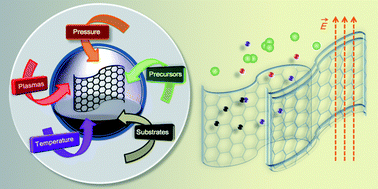
Pity there isn’t a caption. Guess you have to buy the paper for that.
More in Nanoscale
Nanoscale also bills several other graphene papers in the same issue:Another paper turns up in the journal's roster of This week’s HOT articles
In theory
Nice to see the theoreticians are on the case. This in Phys. Rev. Lett. from folks at the Institute for Theoretical Physics at the University of Regensburg.Spin-Orbit Coupling in Hydrogenated Graphene offers “First-principles calculations of the spin-orbit coupling in graphene with hydrogen adatoms in dense and dilute limits”. So now you know.
Laser peels off graphene layers
Thanks to the excellent regime over at IoP Publishing, everyone has 30 days in which to grab the paper Thinning of large-area graphene film from multilayer to bilayer with a low-power CO2 laser from the journal Nanotechnology, a constant source of new papers on graphene. The abstract tells us that “Bilayer graphene has attracted a great deal of attention for many electronic and optical applications”.This paper describes a way of turning the multilayer graphene you get when you make graphene with chemical vapour deposition into a ‘bilayer’ material. This isn’t the first time that people have used layers to thin down graphene, but this time, the researchers claim, the approach “enables high-efficiency thinning of large-area graphene film whilst using a significantly reduced power density and an increased laser beam diameter”.
There’s an interesting connection to Manchester University. This time it isn’t the world famous graphene group that chipped in, but the Laser Processing Research Centre. The graphene expertise seems to have come from Tsinghua University in Beijing.
Graphene on silicon
Another interesting paper over at IoPP is in the open access publication New Journal of Physics, so no need to rush for this one. Strongly confined gap plasmon modes in graphene sandwiches and graphene-on-silicon comes from Imperial College. The researchers have been slapping payers of graphene on top of one another, or, as they put it, “two infinitely long graphene ribbons vertically offset by a gap”.To demonstrate the relevance of their work, the authors report “an unprecedented level of confinement of a terahertz wave of nearly five orders of magnitude when a graphene ribbon is placed on top of a highly doped silicon substrate”. They add that these phenomena and semiconducting substrates “could be the building blocks for both graphene-based integrated optics and ultrasensitive sensing modalities”. Now it just needs someone to do the experiments to show that this is not a mad idea.
14 June 2013
Graphene wired – atom by atom, and other stories
It can take just one chemical bond to make an electrical connection to a graphene ribbon. Researchers at Aalto University in Finland and Utrecht University in the Netherlands did this with “single atom contacts between gold and graphene nanoribbons”.
The researchers describe their work in a paper in Nature Communications, sadly, hidden behind a paywall. Fortunately, the people behind the research are so enthused about their work that they have produced a press release. This points out the small at which graphene electronics can work, less than 10 nanometres. “This means that the graphene nanostructures have to be only a few tens of atoms in width.”
The experiments described in the paper, “Suppression of electron-vibron coupling in graphene nanoribbons contacted via a single atom” showed how to do this. The research involved using atomic force microscopy and scanning tunnelling microscopy “to map the structure of the graphene nanoribbons with atomic resolution”.
The most significant discovery, they say, is that “a single chemical bond forms an electronically transparent contact with the graphene nanoribbon”. They conclude that this finding “may be the key to using graphene nanostructures in future electronic devices, as the contact does not change the intrinsic ribbon properties”.
Tie a graphene ribbon round your battery
Problems with lithium ion (LI) batteries may have given Boeing a headache, but this popular energy store has plenty of fans and down to earth applications. Now researchers at Rice University in Houston, Texas, have come up with a new way of enhancing the efficiency of the LI battery. Their idea, according to the university’s press release, is to employ ribbons of graphene that start as carbon nanotubes.The researchers made anodes out of graphene nanoribbons (GNRs) and tin oxide. (The anode is the bolt hole for the lithium ions, which move to the cathode as the battery discharges.) This novel anode material, “showed an initial capacity better than the theoretical capacity of tin oxide alone”.
It will cost you US$35 to read the paper in ACS Nano, “Graphene Nanoribbon and Nanostructured SnO2 Composite Anodes for Lithium Ion Batteries”. (If it is worth writing a press release, isn’t it also worth providing free access to potential readers?) So we have to rely on what the release says for signs of the true significance of the research. This claims that “After 50 charge-discharge cycles, the test units retained a capacity that was still more than double that of the graphite currently used for LI battery anodes.”
As much as anything, the team sees the work as a testbed for applications of GNRs, a fertile area of research for our wonder material. A member of the group, Jian Lin, a postdoctoral researcher at Rice, describes the research as “starting point for exploring the composites made from GNRs and other transition metal oxides for lithium storage applications.”
The Manchester PR machine rolls on
There was an odd story in the Financial Times this week. The print edition carried the tag “Graphene research” but there wasn’t much of that in sight. The on-line version makes it appear even more graphene oriented, with its title “Graphene breakthrough shows Manchester’s science credentials”. In reality it was mostly a gushing piece about Manchester University and its commercialisation of research that goes on there.The peg for the articles seems to have been the recent press release that we flagged up earlier in the week (see Manchester untied). That was all about magnetism in graphene. Only time will tell us whether or not the paper described there was, as the FT dubs it, another “breakthrough”, but it is certainly a breakthrough in PR. What on earth do we make of the statement that “The university is also home to Professor Brian Cox, the physicist and broadcaster, Sir John Sulston, the Nobel Prize winner who was involved in decoding the human genome, and Jeanette Winterson, the novelist.”
The FT’s article also has some numbers that do not seem to have any relationship with the graphene bit of the story. What do we make of the information that “the university had won £200m in research funding in the first 10 months of the academic year”? How much for graphene?
Then there is the bit that says that the university’s “£32m spin-out fund is funding several attempts to find commercial uses for graphene”. How much of that money has gone into graphene? Can’t they tell us something about those investments?
After all, the writer just needed to read some back issues of the FT. It was on in January that Clive Cookson wrote the article Graphene: Faster, stronger, bendier. This mentioned one of the Manchester businesses, Graphene Industries. Over on the university;s own site, the paper’s journalist could have read the PDF file that describes the launch, last February, of another company, 2-DTech Ltd.
Manchester is a fine university, one of the best, and has an excellent record in knowledge transfer, the sometimes fraught business of getting research into the hands of people who can make money out of it. And you can hardly blame it for the FT’s decision to write something as baffling as this, with its strange mixture of graphene researcher, general university background and throwaway comments from the likes of Eric Schmidt, the chairman of Google.
Heavy metal and the graphene connection
The eyebrows rise when a paper begins “Heavy metal ions and humic acid (HA) in underground water pose a severe threat to public health and ecological systems”. Lots of buzz words in there to appeal to a science watcher. Throw in the title of the paper, “Synergistic Removal of Pb(II), Cd(II) and Humic Acid by Fe3O4@Mesoporous Silica-Graphene Oxide Composites”, and you ask yourself what is graphene doing in there?The paper appears in PLOS One, a peer reviewed open access journal, so anyone can read it and work out for themselves what is going on. It is about hierarchically structured composites containing polyethylenimine-modified magnetic mesoporous silica and graphene oxide (MMSP-GO), whatever they are. The good bit appears to be that “MMSP-GO composites have shown promise for use as adsorbents in the simultaneous removal of heavy metals and humic acid in wastewater treatment processes.”
So you can add cleaning up the environment to graphene’s repertoire.
This blog is a random sample of the many stories on graphene that gush by. Think of it as a poor person's alternative to the expensive newsletters that you can subscribe to from commercial organisations that really do know what they are talking about.
12 June 2013
Spintronics doctors and other graphene stories
The week started well for graphene. No less an accolade than a paper in the Proceedings of the National Academy of Sciences. The trouble comes when you try to make head or tail of the title, Valley Chern numbers and boundary modes in gapped bilayer graphene. It seems to be something to do with topological states and defects.
The researchers at the University of Pennsylvania and the University of Texas at Austin conclude that “gapless interface modes at a LSW are topologically stable when the potential difference between layers is the dominant energy scale and the valley index can be regarded as a good quantum number”. Doubtless this is a truly significant finding for some folks, or it wouldn’t have got into the PNAS. Sadly, the journal does not deem it important enough to have written one of its reader friendly briefs.
Graphene meets silicon
There doesn’t seem to have been much recent graphene activity in Norway, so it is interesting to see a press release on “potential products from the union of semiconductors and graphene”. As the release from The Research Council of Norway puts it “Semiconductors grown on graphene at the Norwegian University of Science and Technology (NTNU) may be the most important research breakthrough of 2012 in Norway.”The release also has an interesting historical anecdote. It seems that the NNTU was put on to the case of graphene six months before the material collected a Nobel prize for its ‘inventors’ and “before graphene had become an item of interest”. A South Korean post-doctoral fellow Dong Chul Kim at NTNU suggested to Helge Weman and Bjørn-Ove Fimland “that they should take a closer look at precisely this material”. The researchers had already grown gallium arsenide nanowires on silicon substrates, so they looked into the possibility of growing semiconductor nanowires on graphene instead. You can follow how they did it in a video on YouTube.
Manchester untied
They are at it again in the labs that brought us graphene. According to the latest press release “a University of Manchester team led by Dr Irina Grigorieva shows how to create elementary magnetic moments in graphene and then switch them on and off”. The report is another part of the armoury of graphene electronics.The news, trailing a paper in Nature Communications, comes with some entertaining notions “Graphene is a chicken wire made of carbon atoms.” On a more scientific note, it quotes Dr Rahul Nair, who led the experimental effort: “Graphene already attracts interest in terms of spintronics applications, and I hope that the latest discovery will make it a frontrunner.”
The media friendly quotes may owe something to the fact that the Manchester team now seems to have a full time communications person. The contact for the story is Daniel Cochlin who is billed as Graphene Communications and Marketing Manager.
07 June 2013
A busy week for four carbon bonds
Where graphene hits the headlines, and other nooks and crannies
Another week, and more news of weird stuff that four carbon bonds can get up to when they get properly organised. Over on the Knowledge Transfer Network (KTN) Materials group they write about Hybrid graphene flame retardants in epoxy improve fire and high temperature performance. Apart from the fact that it is yet another use of our wonder material, the interesting bit is the source of the work. As the KTN write up puts it “Lei Song from University of Science and Technology of China used an in-situ sol-gel process to make organic-inorganic hybrid flame retardants.” The item has a link to the paper in the Journal of Materials Chemistry A, which you’ll have to pay for.The China connection is just another sign of the attention that the local research community is lavishing on us. Of 614 papers that mention graphene in a random selection of publications retrieved over the past decade from the IoPP’s fine library 88 mention the “People’s Republic of China”.
Boiling under
Always nice to see someone finding a new use for graphene, as in another paper from Nature Scientific Reports. Here’s another one with a safety angle. A Novel Role of Three Dimensional Graphene Foam to Prevent Heater Failure during Boiling, describes “a novel boiling heat transfer in reduced graphene oxide suspended in water near critical heat flux, which is traditionally the dangerous limitation of nucleate boiling heat transfer because of heater failure”. The writers claim that this phenomenon “would provide the safer margin of the heat transfer and the amazing impact on the thermal system as the first report of graphene application”. The bottom line, they say, is that “This novel boiling phenomenon can effectively prevent heater failure because of the role played by the self-assembled three-dimensional foam-like graphene network.”Strong stuff
Even engineers of a decidedly mucky nature are muscling in on graphene. Those fine observers of everything manufacturing over at The Manufacturer have found a story from Columbia University. Following the trail we get to the original item “Even with Defects, Graphene Is Strongest Material in the World”. This then leads us to a paper in Science where the more prosaic title “High-Strength Chemical-Vapor–Deposited Graphene and Grain Boundaries” explains why The Manufacturer liked the item. The paper tells us that even graphene of a less than pristine nature – “polycrystalline and thus contain grain boundaries” – is still strong stuff, as strong as the scientifically pure graphene so long as “post-processing steps avoid damage or rippling”.Elephant memory
We’ve been here before it seems. The latest Columbia paper is a follow up to a five-year old publication from the same group that gave us the press release “Columbia Engineers Prove Graphene is Strongest Material”. It was this release that arrived with the quote from James Hone “It would take an elephant, balanced on a pencil, to break through a sheet of graphene the thickness of Saran Wrap.” (This is believed to be a local reference to what Brits might call ‘clingfilm’.)Apple files patent
The newshounds over at New Scientist spotted a patent application from Apple that could see graphene in heat sinks for portable electronic devices. The patent’s claims include:“A method for facilitating the use of a portable electronic device, comprising- arranging a set of components and a battery within an enclosure of the portable electronic device; disposing a heat dissipator comprising graphene over a surface of the battery; and providing thermal contact between one or more of the components and the heat dissipator.”Few patents make it into production. If this one does, will Apple pay taxes on anything that comes from this invention?
Electrodes on the brain
Nanotechnology, the journal, has a more substantial offering on graphene in electronics in The application of graphene as electrodes in electrical and optical devices. With all of the authors working in Korea, where they make electronic stuff by the container load, there’s a better chance that this work, a review of activity in the area, will see light of day. Clearly people are reading this paper: published last year, when we last looked it was number two in the list on the journal’s home page of papers “most read” in the past 30 days.Makes you wonder
Hard to know what to make of this “case study” from EPSRC. no doubt about the subject The wonder stuff but the PDF says no more than the minimal text on the page. there isn’t even a live link to the people the page describes. So we had to get Google to take us to Durham Graphene Science. It turns out to be a spinout from Durham University that has “developed a novel process for the manufacture of high specification graphene”. Smart move: in the early days any money to be made from graphene will go to people making the stuff and selling kit to the research community. Not much in the way of news since 2011 though.A sort of battery
Spinouts are de rigeur for enterprising academics these days. Indeed, it looks like our four carbon bonds have sparked off a new business sector, the graphene battery. There is even a new company out there exploiting their tricks. Graphene Batteries, based in Oslo, “is engaged in development of safe and durable graphene based high energy battery materials”. The idea is to assemble “a key technology IP-portfolio for future licensing and production”.Another company with a finger in the battery business is Lomiko Metals Inc. Lomiko, which has its own graphite mines, recently put out a press release on a collaboration with the Research Foundation of Stony Brook University and Graphene Laboratories, Inc. “to investigate novel, energy-focused applications for graphene” with a specific mention of batteries. The release tells us that “the goal of this collaboration is to map commercially viable routes for the fabrication of graphene-based energy storage devices”.
Graphene Laboratories, based on Long Island, New York, describes itself as “a world leading manufacturer and supplier of graphene products to R&D markets”. So the business reflects the level of maturity, or lack of it, of the graphene market. Perhaps it won’t be long before R&D becomes R, D & D (that’s research, development and demonstration) with the usual order-of-magnitude rise in the costs of projects.
In the picture
There’s another patent application in the works (see Apple above) for a neat use of our slithery carbon bonds, this time from a university group. Laser Focus World tells us that over at Nanyang Technological University (NTU) in Singapore Assistant Professor Wang Qijie has come up with a graphene based image sensor that will allow cameras “to take clear and sharp photos in dim conditions”. The NYU press release optimistically proclaims that we’ll see this development “soon”. The trick was to “create nanostructures on graphene which will “trap” light-generated electron particles for a much longer time, resulting in a much stronger electric signal”.
Professor Wang Qijie slides on graphene that can see in the dark
How facile can you get?
It is always entertaining trying to work out just what the titles of papers mean when they give us a plug. Here’s one that provokes several lines of thought “Facile, scalable synthesis of edge-halogenated graphene nanoplatelets as efficient metal-free eletrocatalysts for oxygen reduction reaction”. It comes from Nature Scientific Reports which, as an open access journal, is free for all to read and ponder.The journal is a regular source of papers about graphene. Here’s one with an intriguing title Highly Sensitive and Selective Gas Sensor Using Hydrophilic and Hydrophobic Graphenes. This time you can see that we are into sensor territory. Oh, yes, the paper’s authors are in Korea.
EuroGRAPHENE’s final fling
They have been thinking about graphene in Strasbourg, where the European Science Foundation (ESF) put together EuroGRAPHENE, “the first coordinated European-wide cooperation on graphene science and technology”. The programme ends this year so the ESF has put together a report on Scientific Highlights (a 2.7 MB PDF file that you can shrink to half that size with the right software!). It lists seven Collaborative Research Projects carried out all over Europe. Well most of Europe, not much in there from the UK.Far from weak ending
The IoPP rounds up a working week of papers with another interesting title Direct writing on graphene 'paper' by manipulating electrons as 'invisible ink. Again, the source is the journal, with authors from the Department of Energy Conversion and Storage at the Technical University of Denmark, and Beijing Key Laboratory of Green Chemical Reaction Engineering and Technology at Tsinghua University.
As the abstract puts it “The combination of self-assembly (bottom up) and nano-imprint lithography (top down) is an efficient and effective way to record information at the nanoscale by writing.” The researchers say that they achieved “Direct high precision microscopic writing on graphene … through an EDX line scan with 1 nm probe in STEM mode”. They sum up their achievements with the observation “These results not only shed new light on an application of graphene concerning the interaction of different forms of carbon but also illuminate the interaction of forms of carbon through an electron beam.”
This is just one of a batch of four papers in the journal. Also check out Control of density and LSPR of Au nanoparticles on graphene, Intrinsic loss due to unstable modes in graphene and Control of density and LSPR of Au nanoparticles on graphene.
14 May 2013
Shale of the century shifts carbon consumption
The rise of shale gas in the US has had unexpected consequences as well as the more obvious effects. It was bound to do wonders for local energy prices, but who would have thought that it would play a part in increasing Germany’s emissions of carbon dioxide?
You can get an idea of shale’s impact on energy markets from a new paper from Chatham House, the Royal Institute of International Affairs. In US Energy: the New Reality John Mitchell reviews recent changes in the energy scene in the US. He shows just how quickly those changes have happened. In 2006, natural gas production in the US reached a low of 18 trillion cubic feet (tcf). (They still use 19th century measurement units there.) By 2012 it had risen by a third to 24 tcf.
The gains for the US are obvious. “Low natural gas prices have expanded the domestic gas market and enhanced the competitiveness of US industries,” says Mitchell. And this will be a long-term effect. Gas-based petrochemical and electricity-intensive industries in the United States “will continue to benefit from cost advantages that are beginning to approach those enjoyed by Middle East petrochemicals industries with oil-related (though discounted) input costs”.
This industrial benefit is in contrast to the UK where last week Sir Alan Rudge, in his farewell address as President of the ERA Foundation, complained that “we are struggling with a disastrous expensive energy policy that is based upon an illusion of a green economy with a huge dependence on imports”. Sir Alan, who has been banging on for some time about the price that industry in the UK has to pay for its energy, lusts after the US’s shale gas. This has, he says, “already reduced energy costs there by a staggering 40 per cent, made them a net exporter of gas, and commenced the rejuvenation of productive industry”.
One consequence of the shale bonanza is, as Sir Alan said, that it has “significantly reduced [CO2] emissions in the USA”. That is because shale gas has half the CO2 content of coal.
This switch from coal to gas in the US has not brought about the dent in CO2 emissions that you might think. It has just exported the carbon for other people to chuck into the atmosphere. One recipient of this carbon looking for a home is Germany.
Mitchell explains what has happened in his paper. Natural gas companies, he points out, have increased their share of the US electricity market by 5 per cent. And it has done this “partly at the expense of coal (which has lost 3 per cent of the electricity generation market)”.
Coal producers haven’t thrown away their picks and shovels and gone on to greener pursuits. They have replaced this loss of domestic sales “by exporting to growing markets in the power sector in Asia and in Europe (the latter reflecting the phasing-out of nuclear power in Germany)”.
So, all those German environmentalists saying no to nuclear power have been bad news for climate change. Yes, Germany is bigger in renewable energy than the rest of Europe, but it still needs to keep the lights on.
23 January 2013
A far from green bamboo computer
How one company’s plans to make a green computer caused a headache for the recyclers.
When the computer company Dell wanted to “go green” it alighted on “bamboo” as a neat environmentally friendly material. Had Dell stuck to what it called" “Nature’s Eco-friendly Packaging Solution” for the boxes that keep hardware safe during transit there might have been no complaints. After all, as it proclaimed, you can just “Toss that Bamboo Packaging into the Compost Pile”.Unfortunately, the company’s designers didn’t stop there. In 2008, they launched what Dell called an “eco computer”, with a case made out of a bamboo based material that looks and behaves just like the ABS polymers used in other computers. You can’t just add that to your vegetable waste and throw it on the compost heap.
Nat Hunter, co-director for Design at the RSA (the Royal Society for the encouragement of Arts, Manufactures and Commerce), tells of going to a recycling plant in Kent. The plant takes old PCs and subjects them to “big rock crushers” – a wrecking ball – to reduce the obsolete computers to piles of rubble, a materials mine.
The waste then goes through sorting line to separate out the different materials for recycling. Unfortunately, Hunter explained at a recent meeting, the sorting system cannot tell the difference between the bamboo plastic and ordinary ABS plastic and shoves it into the same receptacle, thus polluting the real polymer waste.
As Hunter says, the bamboo PC completely failed in its attempts to be ‘eco friendly’. You buy it as a green computer but it ends up being "very problematic" for the recycling industry.
Hunter was talking about Dell’s foray into panda territory at a meeting put on by, among others, the Parliamentary Office of Science and Technology (POST). The meeting, back in January, marked publication of a POST Note Maximising the Value of Recycled Materials. Much of the event – more details here in a piece I wrote for the Materials Research Society in the USA – dealt with the business of recycling plastic, which often entails sorting a pile of mixed polymers, an increasingly sophisticated task made more difficult if the mixture harbours a polymer that masquerades as something else.
Hunter, who is a part of the team behind The Great Recovery – Redesigning the future, a project funded by the Technology Strategy Board, tackled a broader theme, designing manufactured goods to be green from the start. She takes the line that “waste really is a design flaw”.
Designers need to put a lot more effort into thinking about the fate of their products. Dell isn’t the only electronics company in her sights. Hunter, who has spent time watching the recyclers in action, also tells the tale of TVs from Philips that comes with 300 screws holding it together, “all of them different”. By contrast, Samsung makes TVs with half as many screws, all of them the same. Much easier to dismantle.